Samsung’s Metalens Camera Tech Could Usher its Galaxy Devices into a New Era of Ultrathin Phones

Samsung's Metalens technology could revolutionize phone cameras | Representative Image
Samsung has been working on a new optical technology called Metalens in collaboration with Pohang University of Science and Technology (POSTECH). Samsung’s Metalens tech can help in designing smartphones with thinner camera bumps and thinner XR headsets, announced Samsung earlier this year.
Samsung demonstrated Metalens Camera technology that aims to reduce the weight of XR devices and the height of smartphone camera bumps. This tech is a thing of the future that could remove the camera bumps from phones.
Samsung’s and POSTECH’s joint study titled ‘Compact Eye Camera With Two-Third Wavelength Phase-Delay Metalens’ was published in an internationally renowned academic journal called Nature Communications. The study was jointly led by Samsung Research’s Dr. Jeong-Geun Yun and POSTECH professor Junsuk Rho. Hyunjung Kang, a POSTECH researcher, was the co-first author for the study. Samsung did the ideation, implementation, and validation to test the study.
The metalens can manipulate light using nanostructures instead of relying on curved surfaces like traditional lenses. These nanostructures are even thinner than a human hair. Hence, devices that use a metalens can be much thinner and lightweight compraed to current-generation smartphone cameras and XR headsets.
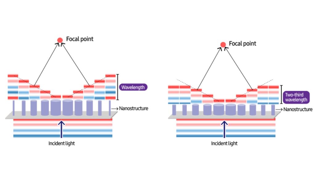
As you can see in the image above, a metalens creates a phase delay of one wavelenght to control light precisely. This is the distance light travels in one oscillation. Phase delay ensures that light waves overlap accurately at the focal point, thereby producing a sharp image.
Utilizing the Metalens technology, Samsung and POSTECH researchers developed an ultra-compact infrared eye camera for XR devices. Metalens reduced the thickness by 20% (from 2.0 mm to 1.6 mm) over refractive-lens cameras.
Technical hurdles
Aspect ratio was the biggest hurdle that was creating roadblocks in the commercialization of Samsung’s Metalens tech. For consumer devices, the camera sensor needs nanostructures with high aspect ratios (at least 1:10).
However, Samsung’s Metalens reduces the required nanostructure aspect ratio to about 1:5. This nanostructure height reduction is made possible without compromising optical performance.
This aspect ratio allows the Metalens to achieve a full-wavelength phase delay for precise light control, making them difficult to fabricate and prone to breakage.
The team, co-led by Dr. Jeong-Geun Yun from Samsung Research and Professor Junsuk Rho from POSTECH, successfully overcame technical limitations.